They can be made any size. Most SATA SSD are just a plastic housing around a board with some chips on it. The right question is when will we have a storage technology with the durability and reliability of spinning magnetized hard drive platters. The nand flash chips used in most SSD and m.2 are much more reliable than they were initially. But for long-term retention Etc. Are still off quite a good bit from traditional hard drives. Hard drives can sit for about 10 years generally before bit rot becomes a major concern. Nand flash is only a year or two iirc.
It’s not the packaging that costs money or limits us, it’s the chips themselves. If we crammed a 3.5” form factor full of flash storage, it would be far outside the budgets of mortals.
Nope. Larger chips, lower yields in the fab, more expensive. This is why we have chiplets in our CPUs nowadays. Production cost of chips is superlinear to size.
Lower storage density chips would still be tiny, geometry wise.
A wafer of chips will have defects, the larger the chip, the bigger portion of the wafer spoiled per defect. Big chips are way more expensive than small chips.
No matter what the capacity of the chips, they are still going to be tiny and placed onto circuit boards. The circuit boards can be bigger, but area density is what matters rather than volumetric density. 3.5" is somewhat useful for platters due to width and depth, but particularly height for multiple platters, which isn’t interesting for a single SSD assembly. 3.5 inch would most likely waste all that height. Yes you could stack multiple boards in an assembly, but it would be better to have those boards as separately packaged assemblies anyway (better performance and thermals with no cost increase).
So one can point out that a 3.5 inch foot print is decently big board, and maybe get that height efficient by specifying a new 3.5 inch form factor that’s like 6mm thick. Well, you are mostly there with e3.l form factor, but no one even wants those (designed around 2U form factor expectations). E1.l basically ties that 3.5 inch in board geometry, but no one seems to want those either. E1.s seems to just be what everyone will be getting.
Not economical. Storage is already done on far larger fab nodes than CPUs and other components. This is a case where higher density actually can be cheaper. ”Mature” nodes are most likely cheaper than the ”ancient” process nodes simply due to age and efficiency. (See also the disaster in the auto industry during covid. Car makers stopped ordering parts made on ancient process nodes, so the nodes were shut down permanently due to cost. After covid, fun times for automakers that had to modernise.)
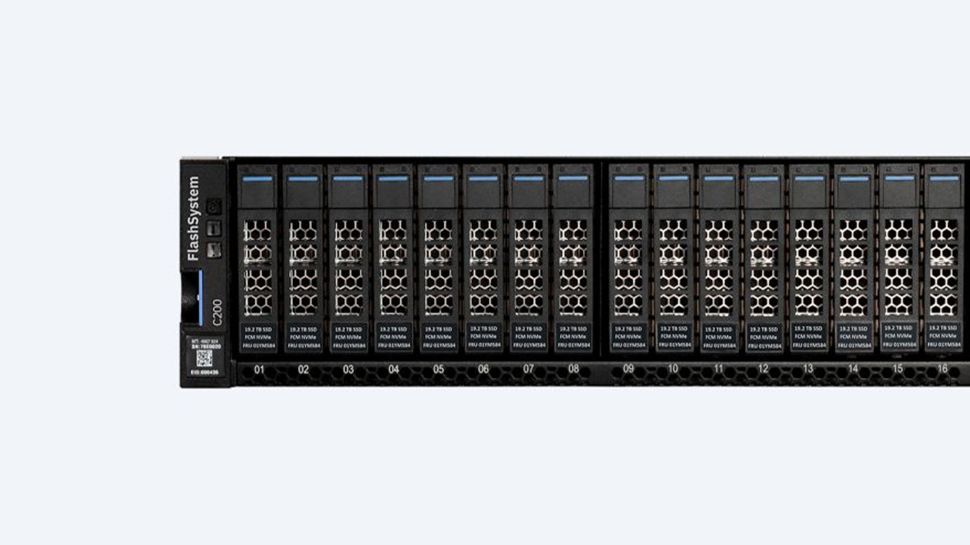
Go compare prices, new NVMe M.2 will most likely be cheaper than SATA 2.5” per TB. The extra plastic shell, extra shipping volume and SATA-controller is that difference. 3.5” would make it even worse. In the datacenter, we are moving towards ”rulers” with 61TB available now, probably 120TB soon. Now, these are expensive, but the cost per TB is actually not that horrible when compared to consumer drives.
I’m not particularly interested to watch a 40 minute video, so I skinned the transcript a bit.
As my other comments show, I know there are reasons why 3.5 inch doesn’t make sense in SSD context, but I didn’t see anything in a skim of the transcript that seems relevant to that question. They are mostly talking about storage density rather than why not package bigger (and that industry is packaging bigger, but not anything resembling 3.5", because it doesn’t make sense).


So can someone make 3.5" SSDs then???
They can be made any size. Most SATA SSD are just a plastic housing around a board with some chips on it. The right question is when will we have a storage technology with the durability and reliability of spinning magnetized hard drive platters. The nand flash chips used in most SSD and m.2 are much more reliable than they were initially. But for long-term retention Etc. Are still off quite a good bit from traditional hard drives. Hard drives can sit for about 10 years generally before bit rot becomes a major concern. Nand flash is only a year or two iirc.
Given that there are already 32TB 2.5” SSDs, what does a 3.5” buy you that you couldn’t get with an adapter?
Native slotting into server drive cages. No concerns about alignment with the front or back.
What kind of server? Dell’s caddies have adapters, and I’m pretty sure some have screw holes on the bottom so you don’t need an adapter.
Why? We can cram 61TB into a slightly overgrown 2.5” and like half a PB per rack unit.
Because we don’t have to pack it in too much. It’d be higher capacities for cheaper for consumers
Also cooling
It’s not the packaging that costs money or limits us, it’s the chips themselves. If we crammed a 3.5” form factor full of flash storage, it would be far outside the budgets of mortals.
You could make the chips bigger, which should be cheaper to produce.
Nope. Larger chips, lower yields in the fab, more expensive. This is why we have chiplets in our CPUs nowadays. Production cost of chips is superlinear to size.
Then lower the storage density. Making things as small as possible almost always ends up being more expensive.
Lower storage density chips would still be tiny, geometry wise.
A wafer of chips will have defects, the larger the chip, the bigger portion of the wafer spoiled per defect. Big chips are way more expensive than small chips.
No matter what the capacity of the chips, they are still going to be tiny and placed onto circuit boards. The circuit boards can be bigger, but area density is what matters rather than volumetric density. 3.5" is somewhat useful for platters due to width and depth, but particularly height for multiple platters, which isn’t interesting for a single SSD assembly. 3.5 inch would most likely waste all that height. Yes you could stack multiple boards in an assembly, but it would be better to have those boards as separately packaged assemblies anyway (better performance and thermals with no cost increase).
So one can point out that a 3.5 inch foot print is decently big board, and maybe get that height efficient by specifying a new 3.5 inch form factor that’s like 6mm thick. Well, you are mostly there with e3.l form factor, but no one even wants those (designed around 2U form factor expectations). E1.l basically ties that 3.5 inch in board geometry, but no one seems to want those either. E1.s seems to just be what everyone will be getting.
Not economical. Storage is already done on far larger fab nodes than CPUs and other components. This is a case where higher density actually can be cheaper. ”Mature” nodes are most likely cheaper than the ”ancient” process nodes simply due to age and efficiency. (See also the disaster in the auto industry during covid. Car makers stopped ordering parts made on ancient process nodes, so the nodes were shut down permanently due to cost. After covid, fun times for automakers that had to modernise.)
Go compare prices, new NVMe M.2 will most likely be cheaper than SATA 2.5” per TB. The extra plastic shell, extra shipping volume and SATA-controller is that difference. 3.5” would make it even worse. In the datacenter, we are moving towards ”rulers” with 61TB available now, probably 120TB soon. Now, these are expensive, but the cost per TB is actually not that horrible when compared to consumer drives.
Relevant video about the problems with high capacity ssds.
https://www.youtube.com/watch?v=Y2i8wZCXDF4
Fourty minutes? Yeah, no. How about an equivalent text that can be parsed in five?
I’m not particularly interested to watch a 40 minute video, so I skinned the transcript a bit.
As my other comments show, I know there are reasons why 3.5 inch doesn’t make sense in SSD context, but I didn’t see anything in a skim of the transcript that seems relevant to that question. They are mostly talking about storage density rather than why not package bigger (and that industry is packaging bigger, but not anything resembling 3.5", because it doesn’t make sense).