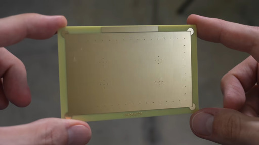
Breadboards are great, but as the world moves more and more to having SMD as a standard, prototyping straight PCBs is becoming more common. If you’re mailing off to China for your PCBs, it’s shockingly quick for what it is, but a one-week turnaround is not “rapid prototyping”. [Stephen Hawes] has been on a quest on his YouTube channel for the ideal rapid-prototyping PCB solution, and he thinks he’s finally got it.
Now, if you’re only doing single-layer PCBs, this is a solved problem. You can mechanically mill, or laser cut, or chemically etch your way to PCB perfection, far faster than the Chinese fabs can get you a part. If you want a double-sided board, however, vias are both a pain in the keister to do yourself, and a rate-limiting step.
You must log in or # to comment.
Nope, but it is an idea. I think he’d be better off with swaging a solid core copper wire. The vast majority of prototypes are primarily constrained by the enclosure. The other main need for vias is to use BGA and other small packages. The types of boards this services can just as easily work as a larger single sided design with jumper wires or resistors, and without the size constraints.
Vias are necessary for literally every part of electronics design beyond the basic I take a premade module and hook it up to these other 2 premade modules (which all have many vias on them), not just small packages.
Most PCBs nowadays are ≥4 layers. You need vias to use the center layers. Vias are necessary for ground return paths, stitching, shielding, RF plane coupling, signal integrity, and much much more. Single layer designing simply does not work if one is actually designing electronics and not just quick and dirty throwing 2 data busses together for a proof of concept.
BGAs don’t need vias, they are so small (0.5mm pitch and smaller) they usually need microvias (0.15mm/0.3mm ID/AR or smaller, which brings PCB prices from 15€ to 300€ for a set). Then the vias generally have to be filled at least and capped, optimally to not suck the solder through the vias from the balls. That is a whole other ballgame.
I etch and design my own boards.
Cool, what does that have to do anything? Are we just swapping facts about ourselves?
I am a professional electronics engineer with experience in high speed data signal integrity analysis, years of circuit and pcb design experience in medical devices, industrial, and consumer electronics with multiple products on the market, and designing and debugging for EMC.
It had to do with your tone and rudeness. Plus you are incorrect in some of your statements, but that is not something I care to address within a place that is about community and being a digital neighbor. The angst reply to a genuine comment is toxic 90s internet that should have died long ago.
Me too mate.
Um, no. That’s just plain incorrect. 🙄
Plenty of useful circuits that are beyond “chuck together a couple of modules” or a “proof of concept” can be implemented on single-sided boards. Look in any hobbyist electronics magazine and you’ll find many of the project designs still use single-sided boards. Many products on the market use single-sided PCBs. My Hakko soldering iron’s control board is single sided. Every PCB in my Sony amplifier is single-sided. The SMPS in almost every LCD monitor, TV and more, exists on a single-sided board.
I would like to see you try to tell the Sony engineers who designed my amplifier that they weren’t “actually designing electronics”, or to the Hakko engineers who designed my soldering iron.
Tell the engineers at Delta that every single switch-mode power supply they ever designed on a single-sided board doesn’t count as “actually designing electronics”.